


The central processing unit (CPU) is the portion of a computer system that carries out the instructions of a computer program, and is the primary element carrying out the computer's functions. The central processing unit carries out each instruction of the program in sequence, to perform the basic arithmetical, logical, and input/output operations of the system.
This term has been in use in the computer industry at least since the early 1960s.[1] The form, design and implementation of CPUs have changed dramatically since the earliest examples, but their fundamental operation remains much the same.
Early CPUs were custom-designed as a part of a larger, sometimes one-of-a-kind, computer. However, this costly method of designing custom CPUs for a particular application has largely given way to the development of mass-produced processors that are made for one or many purposes. This standardization trend generally began in the era of discrete transistor mainframes and minicomputers and has rapidly accelerated with the popularization of the integrated circuit (IC). The IC has allowed increasingly complex CPUs to be designed and manufactured to tolerances on the order of nanometers. Both the miniaturization and standardization of CPUs have increased the presence of these digital devices in modern life far beyond the limited application of dedicated computing machines. Modern microprocessors appear in everything from automobiles to cell phones and children's toys.
History
Computers such as the ENIAC had to be physically rewired in order to perform different tasks, which caused these machines to be called "fixed-program computers." Since the term "CPU" is generally defined as a software (computer program) execution device, the earliest devices that could rightly be called CPUs came with the advent of the stored-program computer.
The idea of a stored-program computer was already present in the design of J. Presper Eckert and John William Mauchly's ENIAC, but was initially omitted so the machine could be finished sooner. On June 30, 1945, before ENIAC was even completed, mathematician John von Neumann distributed the paper entitled First Draft of a Report on the EDVAC. It outlined the design of a stored-program computer that would eventually be completed in August 1949.[2] EDVAC was designed to perform a certain number of instructions (or operations) of various types. These instructions could be combined to create useful programs for the EDVAC to run. Significantly, the programs written for EDVAC were stored in high-speed computer memory rather than specified by the physical wiring of the computer. This overcame a severe limitation of ENIAC, which was the considerable time and effort required to reconfigure the computer to perform a new task. With von Neumann's design, the program, or software, that EDVAC ran could be changed simply by changing the contents of the computer's memory.
While von Neumann is most often credited with the design of the stored-program computer because of his design of EDVAC, others before him, such as Konrad Zuse, had suggested and implemented similar ideas. The so-called Harvard architecture of the Harvard Mark I, which was completed before EDVAC, also utilized a stored-program design using punched paper tape rather than electronic memory. The key difference between the von Neumann and Harvard architectures is that the latter separates the storage and treatment of CPU instructions and data, while the former uses the same memory space for both. Most modern CPUs are primarily von Neumann in design, but elements of the Harvard architecture are commonly seen as well.
As a digital device, a CPU is limited to a set of discrete states, and requires some kind of switching elements to differentiate between and change states. Prior to commercial development of the transistor, electrical relays and vacuum tubes (thermionic valves) were commonly used as switching elements. Although these had distinct speed advantages over earlier, purely mechanical designs, they were unreliable for various reasons. For example, building direct current sequential logic circuits out of relays requires additional hardware to cope with the problem of contact bounce. While vacuum tubes do not suffer from contact bounce, they must heat up before becoming fully operational, and they eventually cease to function due to slow contamination of their cathodes that occurs in the course of normal operation. If a tube's vacuum seal leaks, as sometimes happens, cathode contamination is accelerated. Usually, when a tube failed, the CPU would have to be diagnosed to locate the failed component so it could be replaced. Therefore, early electronic (vacuum tube based) computers were generally faster but less reliable than electromechanical (relay based) computers.
Tube computers like EDVAC tended to average eight hours between failures, whereas relay computers like the (slower, but earlier) Harvard Mark I failed very rarely.[1] In the end, tube based CPUs became dominant because the significant speed advantages afforded generally outweighed the reliability problems. Most of these early synchronous CPUs ran at low clock rates compared to modern microelectronic designs (see below for a discussion of clock rate). Clock signal frequencies ranging from 100 kHz to 4 MHz were very common at this time, limited largely by the speed of the switching devices they were built with.
Discrete transistor and integrated circuit CPUs
The design complexity of CPUs increased as various technologies facilitated building smaller and more reliable electronic devices. The first such improvement came with the advent of the transistor. Transistorized CPUs during the 1950s and 1960s no longer had to be built out of bulky, unreliable, and fragile switching elements like vacuum tubes and electrical relays. With this improvement more complex and reliable CPUs were built onto one or several printed circuit boards containing discrete (individual) components.
During this period, a method of manufacturing many transistors in a compact space gained popularity. The integrated circuit (IC) allowed a large number of transistors to be manufactured on a single semiconductor-based die, or "chip." At first only very basic non-specialized digital circuits such as NOR gates were miniaturized into ICs. CPUs based upon these "building block" ICs are generally referred to as "small-scale integration" (SSI) devices. SSI ICs, such as the ones used in the Apollo guidance computer, usually contained transistor counts numbering in multiples of ten. To build an entire CPU out of SSI ICs required thousands of individual chips, but still consumed much less space and power than earlier discrete transistor designs. As microelectronic technology advanced, an increasing number of transistors were placed on ICs, thus decreasing the quantity of individual ICs needed for a complete CPU. MSI and LSI (medium- and large-scale integration) ICs increased transistor counts to hundreds, and then thousands.
In 1964 IBM introduced its System/360 computer architecture which was used in a series of computers that could run the same programs with different speed and performance. This was significant at a time when most electronic computers were incompatible with one another, even those made by the same manufacturer. To facilitate this improvement, IBM utilized the concept of a microprogram (often called "microcode"), which still sees widespread usage in modern CPUs.[3] The System/360 architecture was so popular that it dominated the mainframe computer market for decades and left a legacy that is still continued by similar modern computers like the IBM zSeries. In the same year (1964), Digital Equipment Corporation (DEC) introduced another influential computer aimed at the scientific and research markets, the PDP-8. DEC would later introduce the extremely popular PDP-11 line that originally was built with SSI ICs but was eventually implemented with LSI components once these became practical. In stark contrast with its SSI and MSI predecessors, the first LSI implementation of the PDP-11 contained a CPU composed of only four LSI integrated circuits.[4]
Transistor-based computers had several distinct advantages over their predecessors. Aside from facilitating increased reliability and lower power consumption, transistors also allowed CPUs to operate at much higher speeds because of the short switching time of a transistor in comparison to a tube or relay. Thanks to both the increased reliability as well as the dramatically increased speed of the switching elements (which were almost exclusively transistors by this time), CPU clock rates in the tens of megahertz were obtained during this period. Additionally while discrete transistor and IC CPUs were in heavy usage, new high-performance designs like SIMD (Single Instruction Multiple Data) vector processors began to appear. These early experimental designs later gave rise to the era of specialized supercomputers like those made by Cray Inc.
Microprocessors
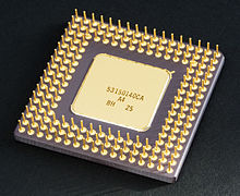
The introduction of the microprocessor in the 1970s significantly affected the design and implementation of CPUs. Since the introduction of the first commercially available microprocessor (the Intel 4004) in 1970 and the first widely used microprocessor (the Intel 8080) in 1974, this class of CPUs has almost completely overtaken all other central processing unit implementation methods. Mainframe and minicomputer manufacturers of the time launched proprietary IC development programs to upgrade their older computer architectures, and eventually produced instruction set compatible microprocessors that were backward-compatible with their older hardware and software. Combined with the advent and eventual vast success of the now ubiquitous personal computer, the term "CPU" is now applied almost exclusively to microprocessors.
Previous generations of CPUs were implemented as discrete components and numerous small integrated circuits (ICs) on one or more circuit boards. Microprocessors, on the other hand, are CPUs manufactured on a very small number of ICs; usually just one. The overall smaller CPU size as a result of being implemented on a single die means faster switching time because of physical factors like decreased gate parasitic capacitance. This has allowed synchronous microprocessors to have clock rates ranging from tens of megahertz to several gigahertz. Additionally, as the ability to construct exceedingly small transistors on an IC has increased, the complexity and number of transistors in a single CPU has increased dramatically. This widely observed trend is described by Moore's law, which has proven to be a fairly accurate predictor of the growth of CPU (and other IC) complexity to date.
While the complexity, size, construction, and general form of CPUs have changed drastically over the past sixty years, it is notable that the basic design and function has not changed much at all. Almost all common CPUs today can be very accurately described as von Neumann stored-program machines. As the aforementioned Moore's law continues to hold true, concerns have arisen about the limits of integrated circuit transistor technology. Extreme miniaturization of electronic gates is causing the effects of phenomena like electromigration and subthreshold leakage to become much more significant. These newer concerns are among the many factors causing researchers to investigate new methods of computing such as the quantum computer, as well as to expand the usage of parallelism and other methods that extend the usefulness of the classical von Neumann model.
Operation
The fundamental operation of most CPUs, regardless of the physical form they take, is to execute a sequence of stored instructions called a program. The program is represented by a series of numbers that are kept in some kind of computer memory. There are four steps that nearly all CPUs use in their operation: fetch, decode, execute, and writeback.
The first step, fetch, involves retrieving an instruction (which is represented by a number or sequence of numbers) from program memory. The location in program memory is determined by a program counter (PC), which stores a number that identifies the current position in the program. In other words, the program counter keeps track of the CPU's place in the program. After an instruction is fetched, the PC is incremented by the length of the instruction word in terms of memory units.[5] Often the instruction to be fetched must be retrieved from relatively slow memory, causing the CPU to stall while waiting for the instruction to be returned. This issue is largely addressed in modern processors by caches and pipeline architectures (see below).
The instruction that the CPU fetches from memory is used to determine what the CPU is to do. In the decode step, the instruction is broken up into parts that have significance to other portions of the CPU. The way in which the numerical instruction value is interpreted is defined by the CPU's instruction set architecture (ISA).[6] Often, one group of numbers in the instruction, called the opcode, indicates which operation to perform. The remaining parts of the number usually provide information required for that instruction, such as operands for an addition operation. Such operands may be given as a constant value (called an immediate value), or as a place to locate a value: a register or a memory address, as determined by some addressing mode. In older designs the portions of the CPU responsible for instruction decoding were unchangeable hardware devices. However, in more abstract and complicated CPUs and ISAs, a microprogram is often used to assist in translating instructions into various configuration signals for the CPU. This microprogram is sometimes rewritable so that it can be modified to change the way the CPU decodes instructions even after it has been manufactured.
After the fetch and decode steps, the execute step is performed. During this step, various portions of the CPU are connected so they can perform the desired operation. If, for instance, an addition operation was requested, an arithmetic logic unit (ALU) will be connected to a set of inputs and a set of outputs. The inputs provide the numbers to be added, and the outputs will contain the final sum. The ALU contains the circuitry to perform simple arithmetic and logical operations on the inputs (like addition and bitwise operations). If the addition operation produces a result too large for the CPU to handle, an arithmetic overflow flag in a flags register may also be set.
The final step, writeback, simply "writes back" the results of the execute step to some form of memory. Very often the results are written to some internal CPU register for quick access by subsequent instructions. In other cases results may be written to slower, but cheaper and larger, main memory. Some types of instructions manipulate the program counter rather than directly produce result data. These are generally called "jumps" and facilitate behavior like loops, conditional program execution (through the use of a conditional jump), and functions in programs.[7] Many instructions will also change the state of digits in a "flags" register. These flags can be used to influence how a program behaves, since they often indicate the outcome of various operations. For example, one type of "compare" instruction considers two values and sets a number in the flags register according to which one is greater. This flag could then be used by a later jump instruction to determine program flow.
After the execution of the instruction and writeback of the resulting data, the entire process repeats, with the next instruction cycle normally fetching the next-in-sequence instruction because of the incremented value in the program counter. If the completed instruction was a jump, the program counter will be modified to contain the address of the instruction that was jumped to, and program execution continues normally. In more complex CPUs than the one described here, multiple instructions can be fetched, decoded, and executed simultaneously. This section describes what is generally referred to as the "Classic RISC pipeline", which in fact is quite common among the simple CPUs used in many electronic devices (often called microcontroller). It largely ignores the important role of CPU cache, and therefore the access stage of the pipeline.
(Theo wiki)