


Operation principle
DRAM is usually arranged in a square array of one capacitor and transistor per cell. The illustrations to the right show a simple example with only 4 by 4 cells (modern DRAM can be thousands of cells in length/width).The long lines connecting each row are known as word lines. Each column is actually composed of two bit lines, each one connected to every other storage cell in the column. (The illustration to the right does not include this important detail.) They are generally known as the + and − bit lines. A sense amplifier is essentially a pair of cross-connected inverters between the bit lines. That is, the first inverter is connected from the + bit line to the − bit line, and the second is connected from the − bit line to the + bit line. This is an example of positive feedback, and the arrangement is only stable with one bit line high and one bit line low.
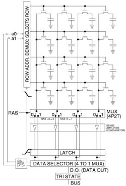
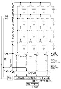
To read a bit from a column, the following operations take place:
- The sense amplifier is switched off and the bit lines are precharged to exactly matching voltages that are intermediate between high and low logic levels. The bit lines are constructed symmetrically to keep them balanced as precisely as possible.
- The precharge circuit is switched off. Because the bit lines are very long, their capacitance will hold the precharge voltage for a brief time. This is an example of dynamic logic.
- The selected row's word line is driven high. This connects one storage capacitor to one of the two bit lines. Charge is shared between the selected storage cell and the appropriate bit line, slightly altering the voltage on the line. Although every effort is made to keep the capacitance of the storage cells high and the capacitance of the bit lines low, capacitance is proportional to physical size, and the length of the bit lines means that the net effect is a very small perturbation of one bit line's voltage.
- The sense amplifier is switched on. The positive feedback takes over and amplifies the small voltage difference until one bit line is fully low and the other is fully high. At this point, the row is "open" and a column can be selected.
- Read data from the DRAM is taken from the sense amplifiers, selected by the column address. Many reads can be performed while the row is open in this way.
- While reads proceed, current is flowing back up the bit lines from the sense amplifiers to the storage cells. This restores (refreshes) the charge in the storage cell. Due to the length of the bit lines, this takes significant time beyond the end of sense amplification, and overlaps with one or more column reads.
- When done with the current row, the word line is switched off to disconnect the storage capacitors (the row is "closed"), the sense amplifier is switched off, and the bit lines are precharged again.
To write to memory, the row is opened and a given column's sense amplifier is temporarily forced to the desired state, so it drives the bit line, which charges the capacitor to the desired value. Due to the positive feedback, the amplifier will then hold it stable even after the forcing is removed. During a write to a particular cell, the entire row is read out, one value changed, and then the entire row is written back in, as illustrated in the figure to the right.
Typically, manufacturers specify that each row should be refreshed every 64 ms or less, according to the JEDEC (Foundation for developing Semiconductor Standards) standard. Refresh logic is commonly used with DRAMs to automate the periodic refresh. This makes the circuit more complicated, but this drawback is usually outweighed by the fact that DRAM is much cheaper and of greater capacity than SRAM. Some systems refresh every row in a tight loop that occurs once every 64 ms. Other systems refresh one row at a time—for example, a system with 213 = 8192 rows would require a refresh rate of one row every 7.8 µs (64 ms divided among 8192 rows). A few real-time systems refresh a portion of memory at a time based on an external timer that governs the operation of the rest of the system, such as the vertical blanking interval that occurs every 10–20 ms in video equipment. All methods require some sort of counter to keep track of which row is the next to be refreshed. Most DRAM chips include that counter; older kinds require external refresh logic to hold that counter. (Under some conditions, most of the data in DRAM can be recovered even if the DRAM has not been refreshed for several minutes.
Memory timing
There are many numbers required to describe the timing of DRAM operation. Here are some examples for two timing grades of asynchronous DRAM, from a data sheet published in 1998:[3]
| "50 ns" | "60 ns" | Description | |
|---|---|---|---|
| tRC | 84 ns | 104 ns | Random read or write cycle time (from one full /RAS cycle to another) |
| tRAC | 50 ns | 60 ns | Access time: /RAS low to valid data out |
| tRCD | 11 ns | 14 ns | /RAS low to /CAS low time |
| tRAS | 50 ns | 60 ns | /RAS pulse width (minimum /RAS low time) |
| tRP | 30 ns | 40 ns | /RAS precharge time (minimum /RAS high time) |
| tPC | 20 ns | 25 ns | Page-mode read or write cycle time (/CAS to /CAS) |
| tAA | 25 ns | 30 ns | Access time: Column address valid to valid data out (includes address setup time before /CAS low) |
| tCAC | 13 ns | 15 ns | Access time: /CAS low to valid data out |
| tCAS | 8 ns | 10 ns | /CAS low pulse width minimum |
Thus, the generally quoted number is the /RAS access time. This is the time to read a random bit from a precharged DRAM array. The time to read additional bits from an open page is much less.
When such a RAM is accessed by clocked logic, the times are generally rounded up to the nearest clock cycle. For example, when accessed by a 100 MHz state machine (i.e. a 10 ns50 ns DRAM can perform the first read in five clock cycles, and additional reads within the same page every two clock cycles. This was generally described as "5‐2‐2‐2" clock), the timing, as bursts of four reads within a page were common.
When describing synchronous memory, timing is described by clock cycle counts separated by hyphens. These numbers represent tCL‐tRCD‐tRP‐tRAS in multiples of the DRAM clock cycle time. Note that this is half of the data transfer rate when double data rate signaling is used. JEDEC standard PC3200 timing is 3‐4‐4‐8 with a 200 MHz clock, while premium-priced high performance PC3200 DDR DRAM DIMM might be operated at 2‐2‐2‐5 timing.
| PC-3200 (DDR-400) | PC2-6400 (DDR2-800) | PC3-12800 (DDR3-1600) | Description | ||||||||||
|---|---|---|---|---|---|---|---|---|---|---|---|---|---|
| Typical | Fast | Typical | Fast | Typical | Fast | ||||||||
| cycles | time | cycles | time | cycles | time | cycles | time | cycles | time | cycles | time | ||
| tCL | 3 | 15 ns | 2 | 10 ns | 5 | 12.5 ns | 4 | 10 ns | 9 | 11.25 ns | 8 | 10 ns | /CAS low to valid data out (equivalent to tCAC) |
| tRCD | 4 | 20 ns | 2 | 10 ns | 5 | 12.5 ns | 4 | 10 ns | 9 | 11.25 ns | 8 | 10 ns | /RAS low to /CAS low time |
| tRP | 4 | 20 ns | 2 | 10 ns | 5 | 12.5 ns | 4 | 10 ns | 9 | 11.25 ns | 8 | 10 ns | /RAS precharge time (minimum precharge to active time) |
| tRAS | 8 | 40 ns | 5 | 25 ns | 16 | 40 ns | 12 | 30 ns | 27 | 33.75 ns | 24 | 30 ns | Row active time (minimum active to precharge time) |
It is worth noting that the improvement over 11 years is not that large. Minimum random access time has improved from tRAC = 50 ns to tRCD + tCL = 22.5 ns, and even the premium 20 ns variety is only 2.5 times better. CAS latency has improved even less, from tCAC = 13 ns to 10 ns. However, the DDR3 memory does achieve 32 times higher bandwidth; due to internal pipelining and wide data paths, it can output two words every 1.25 ns (1600 Mword/s), while the EDO DRAM can output one word per tPC = 20 ns(50 Mword/s).
Timing abbreviations
- tCL – CAS latency
- tCR – Command rate
- tPTP – precharge to precharge delay
- tRAS – RAS active time
- tRCD – RAS to CAS delay
- tREF – Refresh period
- tRFC – Row refresh cycle time
- tRP – RAS precharge
- tRRD – RAS to RAS delay
- tRTP – Read to precharge delay
- tRTR – Read to read delay
- tRTW – Read to write delay
- tWR – Write recovery time
- tWTP – Write to precharge delay
- tWTR – Write to read delay
- tWTW – Write to write delay
Errors and error correction
Electrical or magnetic interference inside a computer system can cause a single bit of DRAM to spontaneously flip to the opposite state. It was initially thought that this was mainly due to alpha particles emitted by contaminants in chip packaging material, but research[6] has shown that the majority of one-off ("soft") errors in DRAM chips occur as a result of background radiation, chiefly neutrons from cosmic ray secondaries, which may change the contents of one or more memory cells or interfere with the circuitry used to read/write them. There was some concern that as DRAM density increases further, and thus the components on DRAM chips get smaller, while at the same time operating voltages continue to fall, DRAM chips will be affected by such radiation more frequently—since lower energy particles will be able to change a memory cell's state. On the other hand, smaller cells make smaller targets, and moves to technologies such as SOI may make individual cells less susceptible and so counteract, or even reverse this trend. Recent studies[7] show that single event upsets due to cosmic radiation have been dropping dramatically with process geometry and previous concerns over increasing bit cell error rates are unfounded.
This problem can be mitigated by using DRAM modules that include extra memory bits and memory controllers that exploit these bits. These extra bits are used to record parity or to use an error-correcting code (ECC). Parity allows the detection of all single-bit errors (actually, any odd number of wrong bits). The most common error correcting code, a SECDED Hamming code, allows a single-bit error to be corrected and (in the usual configuration, with an extra parity bit) double-bit errors to be detected.
Error detection and correction in computer systems seems to go in and out of fashion.[citation needed] Seymour Cray famously said "parity is for farmers" when asked why he left this out of the CDC 6600.[8] He included parity in the CDC 7600, and reputedly said "I learned that a lot of farmers buy computers."[citation needed] The original IBM PC and all PCs until the early 1990s used parity checking.[9] Later ones mostly did not. Wider memory buses make parity and especially ECC more affordable. Many current microprocessor memory controllers, including almost all AMD 64-bit offerings, support ECC, but many motherboards and in particular those using low-end chipsets do not.
An ECC-capable memory controller as used in many modern PCs can typically detect and correct errors of a single bit per 64-bit "word" (the unit of bus transfer), and detect (but not correct) errors of two bits per 64-bit word. Some systems also 'scrub' the errors, by writing the corrected version back to memory. The BIOS in some computers, and operating systems such as Linux, allow counting of detected and corrected memory errors, in part to help identify failing memory modules before the problem becomes catastrophic.
Typically, only machines intended for server use support ECC. Mainboards intended for desktop (rather than server) machines typically do not support ECC, and even those that do support ECC will be shipped with it disabled to allow use of non-ECC memory. Most modern PCs do not support ECC at all as can be seen by examining computer and motherboard specifications; those that do are often supplied with memory modules that do not support parity or ECC. It may be that most users opt for non-ECC systems and memory anyway even when ECC is available. The most important reasons for this are:
- the higher cost of ECC memory (each bank is 9 memory chips compared to 8 for non-ECC memory, and more importantly there is more volume for non-ECC. In some cases the price ratio reduces to 9/8, as an example, on 2008/11/30, on Crucial.com, an ECC CL=5 unbuffered 2GB DDR2-667 DIMM costs $30 while the corresponding non-ECC part costs $28, a difference of 1/15, however some ECC modules cost twice as much as their non-ECC equivalents [Crucial CT12872Z40B and CT12864Z40B, Jan 2009]);
- the higher cost of a motherboard that supports ECC functionality in RAM;
- the additional time needed for ECC memory controllers to perform the error checking and possibly the correction steps, which may lead to an all-around performance hit of around 0.5–2 percent, depending on application;[10] and simple ignorance of the issue.
Error detection and correction depends on an expectation of the kinds of errors that occur. Implicitly, we have assumed that the failure of each bit in a word of memory is independent and hence that two simultaneous errors are improbable. This used to be the case when memory chips were one bit wide (typical in the first half of the 1980s). Now many bits are in the same chip. This weakness does not seem to be widely addressed; one exception is Chipkill.
Recent tests give widely varying error rates with over 7 orders of magnitude difference, ranging from 10−10−10−17 error/bit·h, roughly one bit error, per hour, per gigabyte of memory to one bit error, per century, per gigabyte of memory.
In most computers used for serious scientific or financial computing and as servers, ECC is the rule rather than the exception, as can be seen by examining manufacturers' specifications.
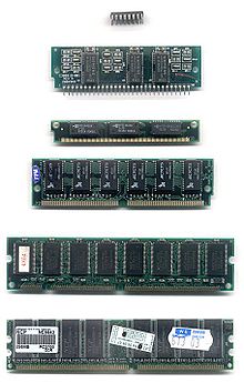
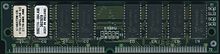
DRAM packaging
For economic reasons, the large (main) memories found in personal computers, workstations, and non-handheld game-consoles (such as Playstation and Xbox) normally consists of dynamic RAM (DRAM). Other parts of the computer, such as cache memories and data buffers in hard disks, normally use static RAM (SRAM).