


Digital Logic Families
Logic families can be classified broadly according to the technologies they are built with. In earlier days we had vast number of these technologies, as you can see in the list below.
- DL : Diode Logic.
- RTL : Resistor Transistor Logic.
- DTL : Diode Transistor Logic.
- HTL : High threshold Logic.
- TTL : Transistor Transistor Logic.
- I2L : Integrated Injection Logic.
- ECL : Emitter coupled logic.
- MOS : Metal Oxide Semiconductor Logic (PMOS and NMOS).
- CMOS : Complementary Metal Oxide Semiconductor Logic.
Among these, only CMOS is most widely used by the ASIC (Chip) designers; we will still try to understand a few of the extinct / less used technologies. More in-depth explanation of CMOS will be covered in the VLSI section.
Basic Concepts
Before we start looking at the how gates are built using various technologies, we need to understand a few basic concepts. These concepts will go long way i.e. if you become a ASIC designer or Board designer, you may need to know these concepts very well.
- Fan-in.
- Fan-out.
- Noise Margin.
- Power Dissipation.
- Gate Delay.
- Wire Delay.
- Skew.
- Voltage Threshold.
Fan-in
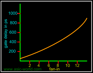
Fan-in is the number of inputs a gate has, like a two input AND gate has fan-in of two, a three input NAND gate as a fan-in of three. So a NOT gate always has a fan-in of one. The figure below shows the effect of fan-in on the delay offered by a gate for a CMOS based gate. Normally delay increases following a quadratic function of fan-in.
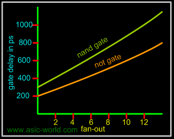
Fan-out
| The number of gates that each gate can drive, while providing voltage levels in the guaranteed range, is called the standard load or fan-out. The fan-out really depends on the amount of electric current a gate can source or sink while driving other gates. The effects of loading a logic gate output with more than its rated fan-out has the following effects. | |
| . | . |
- In the LOW state the output voltage VOL may increase above VOLmax.
- In the HIGH state the output voltage VOH may decrease below VOHmin.
- The operating temperature of the device may increase thereby reducing the reliability of the device and eventually causing the device failure.
- Output rise and fall times may increase beyond specifications
- The propagation delay may rise above the specified value.
Normally as in the case of fan-in, the delay offered by a gate increases with the increase in fan-out.
Gate delay is the delay offered by a gate for the signal appearing at its input, before it reaches the gate output. The figure below shows a NOT gate with a delay of "Delta", where output X' changes only after a delay of "Delta". Gate delay is also known as propagation delay.
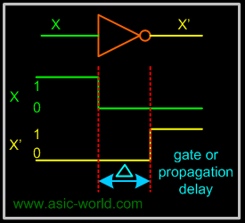
Gate delay is not the same for both transitions, i.e. gate delay will be different for low to high transition, compared to high to low transition.
Low to high transition delay is called turn-on delay and High to low transition delay is called turn-off delay.
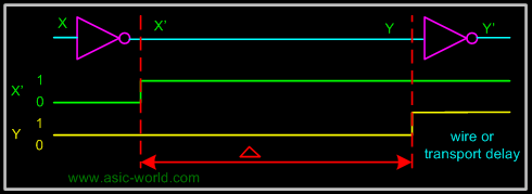
Wire Delay
Gates are connected together with wires and these wires do delay the signal they carry, these delays become very significant when frequency increases, say when the transistor sizes are sub-micron. Sometimes wire delay is also called flight time (i.e. signal flight time from point A to B). Wire delay is also known as transport delay.
Skew
The same signal arriving at different parts of the design with different phase is known as skew. Skew normally refers to clock signals. In the figure below, clock signal CLK reaches flip-flop FF0 at time t0, so with respect to the clock phase at the source, it has at FF0 input a clock skew of t0 time units. Normally this is expressed in nanoseconds.
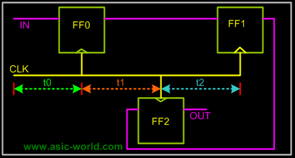
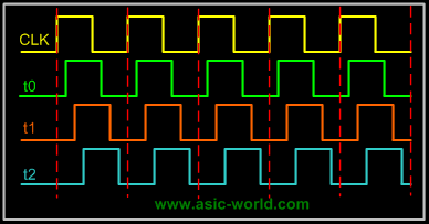
The waveform below shows how clock looks at different parts of the design. We will discuss the effects of clock skew later.
Logic levels are the voltage levels for logic high and logic low.
- VOHmin : The minimum output voltage in HIGH state (logic '1'). VOHmin is 2.4 V for TTL and 4.9 V for CMOS.
- VOLmax : The maximum output voltage in LOW state (logic '0'). VOLmax is 0.4 V for TTL and 0.1 V for CMOS.
- VIHmin : The minimum input voltage guaranteed to be recognised as logic 1. VIHmin is 2 V for TTL and 3.5 V for CMOS.
- VILmax : The maximum input voltage guaranteed to be recognised as logic 0. VILmax is 0.8 V for TTL and 1.5 V for CMOS.
Current levels
- IOHmin: The maximum current the output can source in HIGH state while still maintaining the output voltage above VOHmin.
- IOLmax : The maximum current the output can sink in LOW state while still maintaining the output voltage below VOLmax.
- IImax : The maximum current that flows into an input in any state (1µA for CMOS).
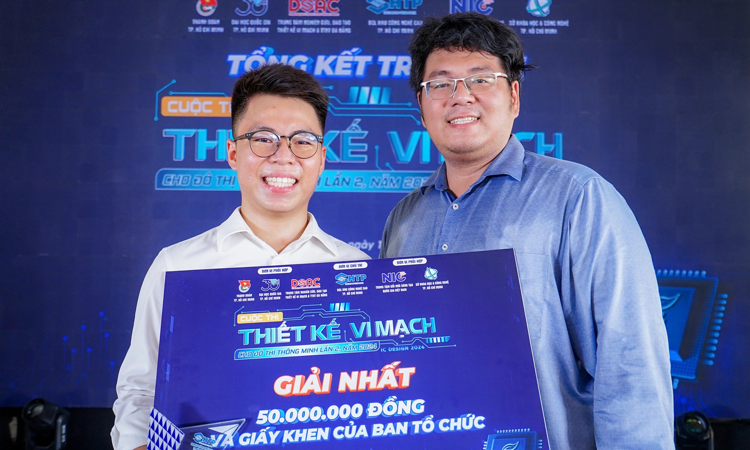
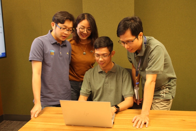
Bạn Có Đam Mê Với Vi Mạch hay Nhúng - Bạn Muốn Trau Dồi Thêm Kĩ Năng
Mong Muốn Có Thêm Cơ Hội Trong Công Việc
Và Trở Thành Một Người Có Giá Trị Hơn
Bạn Chưa Biết Phương Thức Nào Nhanh Chóng Để Đạt Được Chúng
Hãy Để Chúng Tôi Hỗ Trợ Cho Bạn. SEMICON