| | Logic gates have one or more inputs and only one output. The output is active only for certain input combinations. Logic gates are the building blocks of any digital circuit. Logic gates are also called switches. With the advent of integrated circuits, switches have been replaced by TTL (Transistor Transistor Logic) circuits and CMOS circuits. Here I give example circuits on how to construct simples gates. |
| | Symbolic Logic |
| | Boolean algebra derives its name from the mathematician George Boole. Symbolic Logic uses values, variables and operations. |
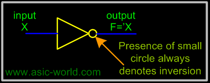
| | Inversion |
| | A small circle on an input or an output indicates inversion. See the NOT, NAND and NOR gates given below for examples. |
| |  |
| | Multiple Input Gates |
| | Given commutative and associative laws, many logic gates can be implemented with more than two inputs, and for reasons of space in circuits, usually multiple input, complex gates are made. You will encounter such gates in real world (maybe you could analyze an ASIC lib to find this). |
| | Gates Types |
| | - AND
- OR
- NOT
- BUF
- NAND
- NOR
- XOR
- XNOR
|
| | AND Gate |
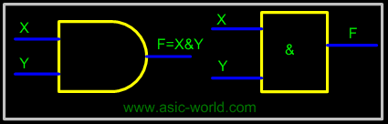
| | The AND gate performs logical multiplication, commonly known as AND function. The AND gate has two or more inputs and single output. The output of AND gate is HIGH only when all its inputs are HIGH (i.e. even if one input is LOW, Output will be LOW). |
| | If X and Y are two inputs, then output F can be represented mathematically as F = X.Y, Here dot (.) denotes the AND operation. Truth table and symbol of the AND gate is shown in the figure below. |
| | Symbol |
| |  |
| | Truth Table |
| | | X | Y | F=(X.Y) | | 0 | 0 | 0 | | 0 | 1 | 0 | | 1 | 0 | 0 | | 1 | 1 | 1 | |
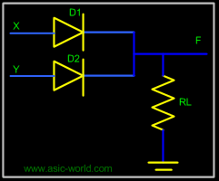
| | Two input AND gate using "diode-resistor" logic is shown in figure below, where X, Y are inputs and F is the output. |
| | Circuit |
| | 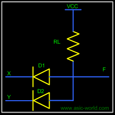 |
| | If X = 0 and Y = 0, then both diodes D1 and D2 are forward biased and thus both diodes conduct and pull F low. |
| | If X = 0 and Y = 1, D2 is reverse biased, thus does not conduct. But D1 is forward biased, thus conducts and thus pulls F low. |
| | If X = 1 and Y = 0, D1 is reverse biased, thus does not conduct. But D2 is forward biased, thus conducts and thus pulls F low. |
| | If X = 1 and Y = 1, then both diodes D1 and D2 are reverse biased and thus both the diodes are in cut-off and thus there is no drop in voltage at F. Thus F is HIGH. |
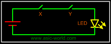
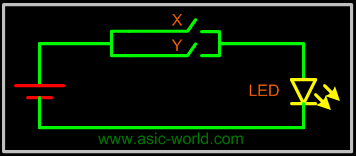
| | Switch Representation of AND Gate |
| | In the figure below, X and Y are two switches which have been connected in series (or just cascaded) with the load LED and source battery. When both switches are closed, current flows to LED. |
| |  |
| | Three Input AND gate |
| | Since we have already seen how a AND gate works and I will just list the truth table of a 3 input AND gate. The figure below shows its symbol and truth table. |
| | Circuit |
| | 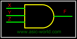 |
| | Truth Table |
| | | X | Y | Z | F=X.Y.Z | | 0 | 0 | 0 | 0 | | 0 | 0 | 1 | 0 | | 0 | 1 | 0 | 0 | | 0 | 1 | 1 | 0 | | 1 | 0 | 0 | 0 | | 1 | 0 | 1 | 0 | | 1 | 1 | 0 | 0 | | 1 | 1 | 1 | 1 | |
| | OR Gate |
| | The OR gate performs logical addition, commonly known as OR function. The OR gate has two or more inputs and single output. The output of OR gate is HIGH only when any one of its inputs are HIGH (i.e. even if one input is HIGH, Output will be HIGH). |
| | If X and Y are two inputs, then output F can be represented mathematically as F = X+Y. Here plus sign (+) denotes the OR operation. Truth table and symbol of the OR gate is shown in the figure below. |
| | Symbol |
| | 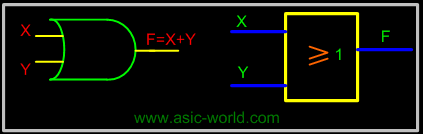 |
| | Truth Table |
| | | X | Y | F=(X+Y) | | 0 | 0 | 0 | | 0 | 1 | 1 | | 1 | 0 | 1 | | 1 | 1 | 1 | |
| | Two input OR gate using "diode-resistor" logic is shown in figure below, where X, Y are inputs and F is the output. |
| | Circuit |
| |  |
| | If X = 0 and Y = 0, then both diodes D1 and D2 are reverse biased and thus both the diodes are in cut-off and thus F is low. |
| | If X = 0 and Y = 1, D1 is reverse biased, thus does not conduct. But D2 is forward biased, thus conducts and thus pulling F to HIGH. |
| | If X = 1 and Y = 0, D2 is reverse biased, thus does not conduct. But D1 is forward biased, thus conducts and thus pulling F to HIGH. |
| | If X = 1 and Y = 1, then both diodes D1 and D2 are forward biased and thus both the diodes conduct and thus F is HIGH. |
| | Switch Representation of OR Gate |
| | In the figure, X and Y are two switches which have been connected in parallel, and this is connected in series with the load LED and source battery. When both switches are open, current does not flow to LED, but when any switch is closed then current flows. |
| |  |
| | Three Input OR gate |
| | Since we have already seen how an OR gate works, I will just list the truth table of a 3-input OR gate. The figure below shows its circuit and truth table. |
| | Circuit |
| |  |
| | Truth Table |
| | | X | Y | Z | F=X+Y+Z | | 0 | 0 | 0 | 0 | | 0 | 0 | 1 | 1 | | 0 | 1 | 0 | 1 | | 0 | 1 | 1 | 1 | | 1 | 0 | 0 | 1 | | 1 | 0 | 1 | 1 | | 1 | 1 | 0 | 1 | | 1 | 1 | 1 | 1 | |