Over the years, design complexity and size have stubbornly obeyed the growth curve predicted by Intel co-founder Gordon Moore. Moore stated that the number of transistors on integrated circuits doubles approximately every two years. The chip makers want to pack as many functions as possible in their SoCs and provide as many feature additions to gain market share. The additional features increase the complexity and effort for verification.
A study suggests that the key industry trends in the global chip design market are the escalating cost of chip design, increasing design complexity, and shorter market time for new products. The worst thing that could happen to a chipset company is a respin due to a functional bug in the product. This calls for a greater concerted effort to verify complex designs in minimal time and a particular need for skilled and smart verification resources to reduce development costs. This article covers the minimum scope and some guidelines for efficient verification methodology for today’s SoCs.
Key concerns for verifying SoCs
There’s always the option to deploy more resources to verify the complex design in less cycle time assuming that there are enough resources present in the industry, but this will also lead to an increase in the manufacturing cost. This is not good for a company in terms of gross margins. So in this case, the main question that arises is “What to verify at SoC level?”
For this, one must understand the basic difference between SoC verification and intellectual property (IP) verification. While designing an SoC, IP is generally delivered by a third party, or it is developed in-house and we can assume it has been verified by the IP level verification test-suite. The SoC team integrates the IP as per the defined functionalities in the specifications. Then, the SoC verification team has to verify the chip-level functionality, which mainly focuses on the integration of IP. Each IP block supports many features, so it is very important to understand which features need to be verified at the SoC level. For Example, an IP block can have a number of interrupt outputs, but the SoC team can only verify the interrupts that are connected at the SoC level.
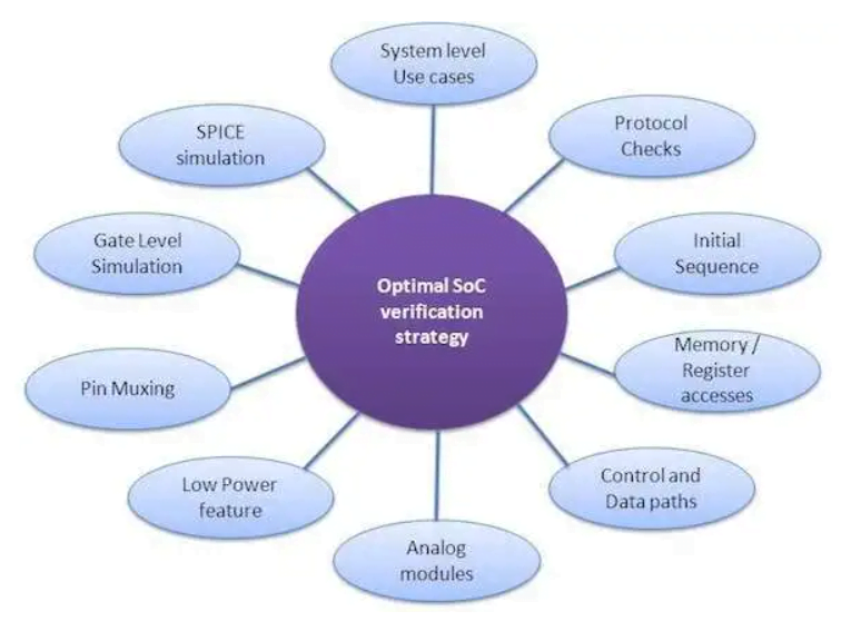
Important areas during SOC verification.
Some important concerns during SoC level verification include:
- Pin muxing in the chip: The number of pins in a SoC is directly related to the chip cost and determined by customer requirements, so the SoC is restricted with limited pins as compared to the number of pins required by IP to interface to the external world. In order to use the SoC pins efficiently, they are interfaced to the internal IP via a complex muxing logic at the SoC level. It is very important to verify this logic.
- Protocol checks: Protocol checkers should be added at module boundaries.
- Initial sequences for the SoC bringup: This mainly includes the reset and boot-up sequences. Apart from reset sequence checking, a typical SoC can have multiple ways to boot-up , e.g. from internal or external memory. Checking the boot from all possible sources can be one area of focus.
- Memory and register access: Focus here can be to ensure that design can configure registers and memory to enable various SoC level scenarios.
- Control and data paths in the design: The focus here is to cover datapaths that involve configuring transactions with the external world (interface protocols at SoC like LIN, CAN, UART, etc.), configure masters of transactions to work in parallel (processor, DMA etc), and excitation of functional paths for interrupts.
- Analog modules: Special focus on analog block integration verification is needed as traditional digital verification may not model analog behavior properly. It is recommended that behavioral models for analog modules be written in VAMS (Verilog-AMS) in order to emulate behavior on silicon as closely as possible.
- Low power feature: Low power is an important feature in the SoC because it is a key requirement for applications like energy metering, smart phones or tablets. Tests should check low power entry and exit. With the advanced simulation techniques of verifying low power intent (like CPF or UPF), these patterns can verify low power intent with the addition of low power structures like isolation cells or level shifters at the RTL stage itself.
- Polarity check: Polarity of the connection of the output port of one module to the input port of the other module.
- Gate level simulation: The point here is to catch timing related issues, constraint validation glitches, combinational logic on reset path, etc.
- SPICE simulations: These are used to verify the analog functionality in the chip. Digital simulation may be limited by the accuracy of behavioral models of analog blocks and the limitations of modeling analog behaviur in traditional HDL languages. SoC simulations can be run with few analog blocks in SPICE and the rest of the system in digital to verify analog block integration.
- System level use cases: Special consideration needs to be given to the application-level use cases that excite the control and data paths for multiple applications running in parallel. These are the application scenarios that the customer will finally run on the SoCs and adds confidence in verification. This can be targeted to find any bottleneck in the design, such as processor latency, DMA path latency, and/or interrupt priorities in customer use cases.
Efficient Verification Strategy
As per the VLSI industry trend, the complexity of the chips is increasing while cycle time is reducing. So, even after so much planning on “what to verify,” it may still not be possible to verify upcoming complex designs. As a result, designers need to plan for automation needs in the verification cycle to help verify the entire design while maintaining quality standards and on-time delivery.
The following steps can help to make the verification process more efficient:
Effectiveness of the test-suite: The verification plan should be made from the system-level architecture document (Chip Spec) so that each feature mentioned in the Chip Spec is mapped to at least one test pattern in the verification suite. The test patterns must be reviewed and checked for the feature (verified by that pattern) and map it to the corresponding feature in the Chip Spec. The test patterns must contain proper comments, as per the pattern intent.
Automatic test-pattern generation: Tests that check basic features (like the memory and the register access) can be generated through automation.
Self-checking patterns: Test patterns must check the intended functionalities and should indicate pass or fail, depending on the checks intended. Some of the checks could be to verify the number of interrupts that occurred vs expected or expected values of the status register at end of a transaction. Having automated checks can save a lot of debugging time on failures.
Automated checks in Testbench: Monitors and assertions should be enabled in the testbench to perform automated checks for key functionalities. Clock monitors and low power mode entry sequences are a few of the checks that can be helpful.
Reusable test-suite: A verification test-suite should be made in such a way that it is fully reusable. That way, for every new SoC it is simply a plug and plays with some minor adjustments in case there are some new features of that IP that is to be used in the SoC. Test cases should be coded in a high-level language so that they are independent of the processor and easily reusable for different SoCs. This avoids the extra effort of test-suite creation every time an SoC changes and reduces the verification cycle time. Test suite reuse could be of two types: horizontal (SoC to SoC) or vertical (IP to SoC). Both enhance efficiency.
Leverage pre-silicon platform: It takes a lot of simulation time for the long patterns to run in a verification environment. To improve cycle time, the verification plan must identify key scenarios that have very large simulation times to be run on the pre-silicon platform.
Randomization: Use randomization in the test bench for hitting the corner cases in the design. Some of the parameters that can be randomized are:
• Values written in the register’s read/write patterns
• Number of resets to be given in the pattern
• Pin used for wakeup from low-power mode
• Latency in the wakeup from low-power mode
• Wakeup pulse duration
The following help hit the corner cases that may be difficult to target in a directed scenario:
- Intelligent pattern selection for gate-level simulations: Gate-level simulations are very slow as compared to RTL simulations, so the test pattern suite should be selected carefully. For example, all of the patterns that are part of the RTL simulation need not be run at gate level. Target those patterns that exercise IO paths, digital-analog interactions, clock gating and clock switching muxes for glitch detection etc.
- Regressions: SoC level regressions must be enabled at very early stages in the verification cycle to review progress against overall test completion.
- IP Level regressions: An IP level regression suite must be run on IP releases delivered to the SoC team, so that the SoC team can focus on SoC level defects.
- Formal verification of IOMuxing: Efficently verify the IO path. As there are limited pins on chip and with increasing logic in chip, the number of functionalities muxed on each pin are increasing. So, covering all of the paths by directed patterns might not be possible. Formal checks can be done for IOMuxing verification as a quick and efficient method.
- Coverage: Design coverage (Toggle, Code, FSM) must be enabled to collect the coverage data in each regression run so as to see the coverage holes and cover them. This ensures that you are progressing towards the end goal. Add the cover points and cover groups for that cover points in the testbench and collect the functional coverage to check whether all the assertions and monitors are covered as per the test-suite.
- Low power feature: Verify in both RTL and gate level simulations in order to ensure proper low power cells insertion in the design.
When to Stop?
This is the question that arises in the mind of every verification engineer while giving the sign-off on a design. Indeed, it is an important one. Here are a few pointers. Even if gate count increases linearly, the possible states in design may increase exponentially. It may not be possible to verify all possible states of the design. A clearly defined set of coverage goals ensures that the verification efforts are focused on convergence with quality in a limited time. Module-level verification enables coverage data collection at the IP level. Complete code coverage (line, expression, block, FSM, and toggle) reports can be generated at the module level. Functional coverage and assertion coverage data can also be collected at this level as well.
For SoC level integration checks, the toggle coverage can be an important metric. The code coverage (line, expression, block) for logic coded by the SoC team (like clocking logic, some glue logic, etc) should be reviewed and analyzed thoroughly in order to cover all of the required logic in the verification. It can help to enhance the test suite that covers the gaps. Functional coverage can also be collected for the assertions so as to check that all the sequences have happened correctly.
For analog components, one can define functional coverage and assertions for the behavioral models to ensure that the regular operating modes are verified. For low-power modes coverage, the power format files can be easily used to collect a functional coverage database of low-power states. This coverage closure (no holes left as per specifications) ensures that we have not missed anything in respect to the verification of design functionality.
Bạn Có Đam Mê Với Vi Mạch hay Nhúng - Bạn Muốn Trau Dồi Thêm Kĩ Năng
Mong Muốn Có Thêm Cơ Hội Trong Công Việc
Và Trở Thành Một Người Có Giá Trị Hơn
Mong Muốn Có Thêm Cơ Hội Trong Công Việc
Và Trở Thành Một Người Có Giá Trị Hơn
Bạn Chưa Biết Phương Thức Nào Nhanh Chóng Để Đạt Được Chúng
Hãy Để Chúng Tôi Hỗ Trợ Cho Bạn. SEMICON